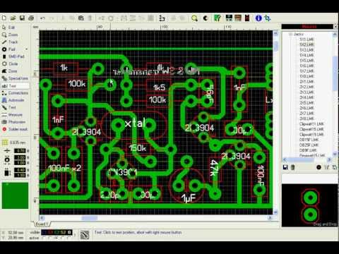
How to manually trace a PCB artwork with Sprint Layout.
Август 14, 2014
Here is a short video demo on how to manually trace a PCB artwork/image with Sprint Layout.
There are instances that we want to create a PCB from circuit or layout we found on Internet but don't have the actual PDF file or correct size for DIY production. With this powerful feature of Sprint Layout PCB design software, we can manually trace a scanned copy or image of PCB artwork.
21 3
7,075 просмотров

PCB Fabrication Process Tour
Step-by-step tour of domestic manufacturer Saturn Electronics Corporation metro Detroit board house detailing the various processes involved in the fabrication of a bare printed circuit board.
979 84

Making of PCBs at home, DIY using inexpenive materials
An easily understandable video demonstration of how to make PCBs(Fabricate) at home with available inexpensive materials using toner transfer method.
Requirements for making PCB are Plain copper coated board, Ferric Chloride, PCB hand drill, Hacksaw blade, Iron box, LASER printer(not inkjet) and Glossy paper [photo paper].
Here Cadsoft Eagle has been used to design board layout, any other CAD tools can also be used.Acetone[nail polish remover] can be used to clean copper surface. Immerse the board for a sufficient time in boiling water for peeling off the paper.While peeling slowly remove the paper from borders don't remove it rapidly since toner might also get removed. If you miss the continuity in the toner mask or if toner gets distorted [path or any small area of design] while peeling off the paper use Permanent marker[like CD maker] to manually draw the path before etching, wash the toner transferred board with plain water and make it dry before drawing with Permanent marker. For fast etching stir the Ferric Chloride solution for every 2 minutes.Air pump agitator[like aquarium air pump] also speeds up the etching process by bubbling through the solution and warm solution can also be used for doing this.
The board made in this video is for object tracking robot using Atmega328p and Xbee Pro.
Thanks to Rashmi..
6069 270

DIY Printed circuit board
My personal experience with heat toner transfer method of making PCB. It works ONLY with laser printer.
Purpose of chemical tinning in last step is to protect copper against oxidation and provide good solderability.
Using Liquid tin is optional. Tinning can be done manually with regular solder, flux and iron.
All chemicals used in PCB manufacturing should be available at electronic hobby shop or can be found online.
There's list of product distributors at manufacturer's web site
http://www.mgchemicals.com/distributors/index.html
My DIY tutorials and fun projects at
http://www.apdigitallight.com/
3332 208

Checkerboard pattern for magnetic levitation
This video is part of my series on how to handle neodymium magnets safely.
This is a more advanced lesson on how to make a matrix of magnets with the poles in a checkerboard pattern. This is what you need to make a piece of diamagnetic pyrolytic graphite levitate. I will also give you some hints on how to take the matrix apart again.
Here are the captions in case the combination of my lousy microphone and danish accent is hard to understand (also available: danish and english closed captions — just press the CC button under the video):
Hello there, this video is part of my series on how to handle neodymium magnets safely.
In this video I am showing you how to safely put together magnets with the poles in a checkerboard pattern that is suitable for levitation.
What you see is pyrolytic graphite being repelled by four neodymium magnets.
So let's start with some tiny ones. These can be arranged by hand alone but don't for a second think they are weak. Just one of these will hold over a kilogram of iron.
The only tool I recommend for these tiny magnets is this simple locking-board.
The iron plates underneath locks the loose magnets in place — or at least dampens the acceleration when putting the magnets together.
These thin magnets are very fragile and will easily break if just thrown together.
Alright. Here's the checkerboard pattern of north and south poles I am going to make.
Let's go ahead and take the first magnet of the stack and place it on the locking board. The next magnet you need to turn 180 degrees before putting it on.
The poles of the magnets can't face in the same direction since only opposites attracts.
Continue doing this and remember to turn every second magnet upside down.
There you go...
And now just some hints for restacking the magnets without breaking them.
OK — what you've seen so far may be basic to most of you so let me raise the ante.
These are tricky little bastards. They are just the size where they don't look impressive like a huge one in some of my other videos but these will draw blood if you get pinched by them.
Who said nerds don't work out? :)
I have marked the north poles on these cube magnets with dots around the edges so I always
know which two surfaces are the poles.
Let's build a checkerboard: take the first magnet of the stack using a splitter tool.
Put the magnet on the locking board with one of the pole surfaces pointing upwards.
For the next magnet you need a large wedge to slide the two magnets safely together.
Remember to turn the next magnet upside down so you've got opposite poles attracting
each other.
I will make a 3x3 pattern so let me just put another one on — mind the poles.
Repeat until you have three of these 3x1 bars. Remember to keep them far apart so they don't smash together.
Take one of the bars and mind the poles.
Take the next bar and put it upside down on the locking board following the rule of attraction
between opposite poles.
Bring the bars together with the wedge in between and make sure the bars are aligned.
Finish the project with the last bar.
There you have it: nine powerful magnets put together with no loss of blood.
And here's what they can do.
Now for some hints on how I restack them. As always: Mind the poles... Bye bye for now.
1769 28

How to create Sprint Layout macros
Creating user-defined macros in Sprint Layout 6.0
5 2

Altium Designer Tutorial: Schematic capture and PCB layout (2of2)
A simple tutorial on how to use the schematic and PCB functionality of Altium Designer.
1123 30


How to make PCB using MARKER PEN (Printed Circuit Board)
How to make PCB using MARKER PEN (Printed Circuit Board)
Please Like & Share. Thanks for subscribe.
http://diy-project.org
Subscribe Here because amazing videos will come soon: https://www.youtube.com/c/DIYProjectsideas?sub_confirmation=1
Visit DIY Projects Channel for more Cool Videos
https://www.youtube.com/c/DIYProjectsideas
© 2018 DIY Projects All Rights Reserved
A printed circuit board, or PCB, is used to mechanically support and electrically connect electronic components using conductive pathways, tracks or signal traces etched from copper sheets laminated onto a non-conductive substrate. When the board has only copper tracks and features, and no circuit elements such as capacitors, resistors or active devices have been manufactured into the actual substrate of the board, it is more correctly referred to as printed wiring board (PWB) or etched wiring board. Use of the term PWB or printed wiring board although more accurate and distinct from what would be known as a true printed circuit board, has generally fallen by the wayside for many people as the distinction between circuit and wiring has become blurred. Today printed wiring (circuit) boards are used in virtually all but the simplest commercially produced electronic devices, and allow fully automated assembly processes that were not possible or practical in earlier era tag type circuit assembly processes.
Just in 5 simple steps
A PCB populated with electronic components is called a printed circuit assembly (PCA), printed circuit board assembly or PCB Assembly (PCBA). In informal use the term "PCB" is used both for bare and assembled boards, the context clarifying the meaning. The IPC preferred term for populated boards is CCA, circuit card assembly.[1] This does not apply to backplanes; assembled backplanes are called backplane assemblies by the IPC.
Alternatives to PCBs include wire wrap and point-to-point construction. PCBs must initially be designed and laid out, but become cheaper, faster to make, and potentially more reliable for high-volume production since production and soldering of PCBs can be automated. Much of the electronics industry's PCB design, assembly, and quality control needs are set by standards published by the IPC organization.
how to make PCB using marker pen
how to make pcb at home
© 2013 HadronMesons All Rights Reserved
Benyamin Amiri
851 124
Sprint Layout Drawing
I have made some video when i was drawing some project in Sprint Layout 5.0
38 11

High Speed PCB Design Rules (Lesson 4 of Advanced PCB Layout Course)
5 most common High Speed Design rules. Find the complete course at: http://www.fedevel.com/academy
837 16
